Unlike their three-dimensional configuration, two-dimensional materials with "all atoms exposed on the surface" allow for Atom-by-Atom precise structure resolution and reveal new conformational relationships at the atomic scale in two dimensions. Through bottom-up precision growth control and top-down artificial stacking fabrication, our research interests are focused on light-element quantum materials and their heterostructures, exploring their intrinsic electrical, optical, and thermal properties, as well as their regulatory tools and potential applications.
————————————————————————————————————————————————————————
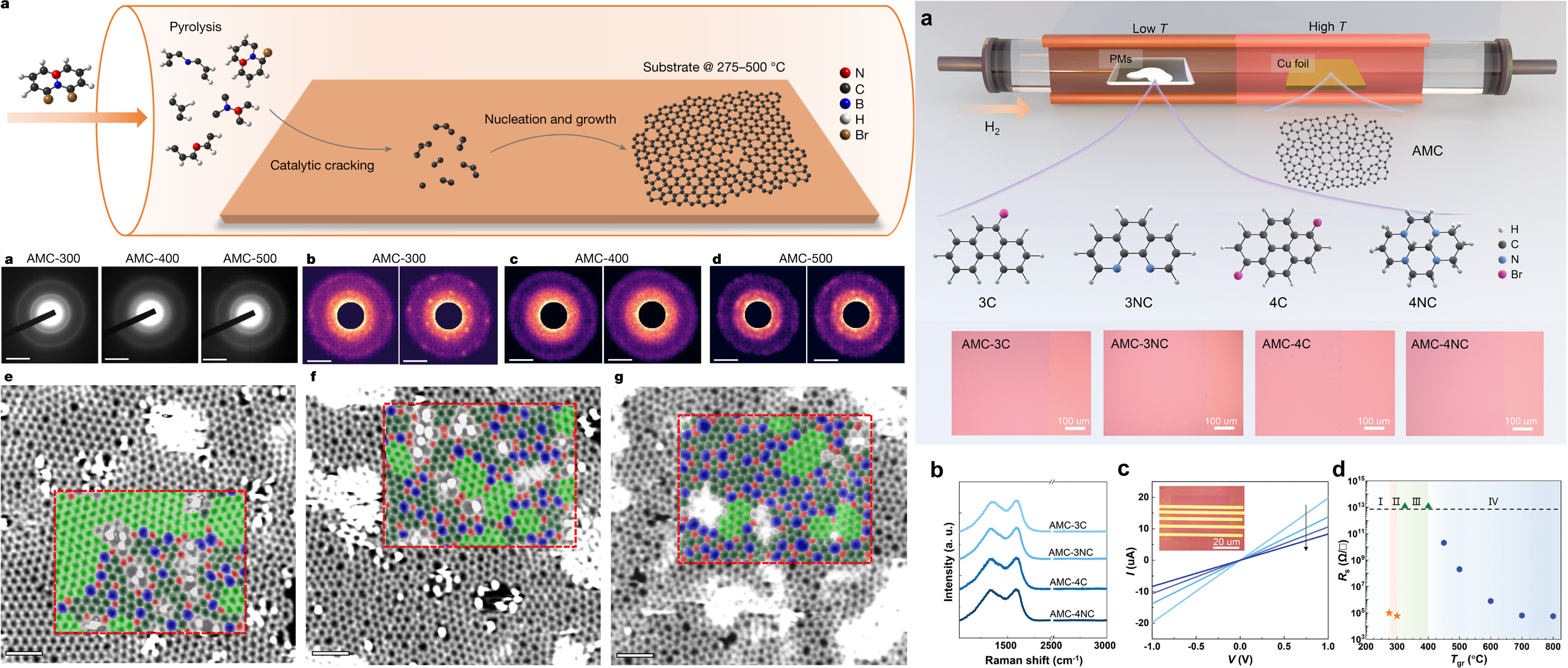
In the study of three-dimensional amorphous materials, the lack of long-range atomic order and direct observation methods has obscured their packing and topological configurations. A long-standing challenge in materials science lies in establishing atomic-level structure-property relationships for such disordered systems, a problem highlighted among the 125 frontier scientific questions by Science magazine. Addressing this, the applicant developed a chemical vapor deposition (CVD) method to synthesize atomically thin 2D amorphous carbon with tunable disorder, enabling quantitative correlation between atomic arrangements and electronic properties (Nature 2023, 615, 56).
By utilizing heteroatom-containing organic precursors at low growth temperatures (as low as 275 °C), crystalline phases were suppressed. Atomic-resolution TEM revealed a unique microstructure: distorted hexagonal domains embedded in a disordered network of 5-8-membered rings, termed "topological disorder." Electrical measurements demonstrated a nine-order-of-magnitude tunability in conductivity via temperature control. Combining structural analysis, device characterization, and theoretical modeling, two structural parameters—medium-range order and hopping island density—were identified as critical descriptors for correlating microscopic disorder with macroscopic conductivity, establishing a comprehensive "phase diagram." Further work extended the synthesis to commercial precursors, confirming the universality of disorder-governed conduction, consistent with N.F. Mott's variable-range hopping theory. This work not only resolves fundamental questions about structure-function relationships in amorphous materials within a simplified 2D framework but also opens avenues for designing disordered 2D materials with tailored electronic properties (Adv. Funct. Mater. 2025, 2424751).

————————————————————————————————————————————————————————
Mass disorder, a rarely explored yet critical and ubiquitous form of disorder, arises from isotopic variations where elements share the same proton count but differ in neutron numbers. Unlike natural isotopic distributions, isotope engineering enables controllable synthesis of samples with purified or tunable isotope ratios, defining a novel structural parameter termed "mass order." Its effects in 2D materials remain largely unknown.
Focusing on isotope-purified hexagonal boron nitride (h-BN), the applicant pioneered a single-component metal-flux method to synthesize large-area (cm²-scale) continuous h-BN films, achieving isotopically purified h-10BN and h-11BN. Thermal conductivity measurements revealed a record-high value in h-11BN, demonstrating enhanced phonon transport upon eliminating mass disorder. In WS₂/h-BN heterostructures, isotope engineering, alongside temperature and pressure, modulated interlayer electron-phonon coupling, uncovering unprecedented isotope-dependent Raman features unexplained by existing theories. Additionally, isotope engineering in hydrogenated germanene (Ge-H/Ge-D) effectively tuned lattice vibrations, optical bandgaps, and interlayer spacing. By establishing isotope engineering as a new structural degree of freedom in 2D materials, this work reveals exotic physical phenomena in isotopically tailored systems. Practically, the synthesized high-quality, isotope-tunable h-BN films show promise for thermal management (high-conductivity fillers) and thermal neutron detection (via 10B’s large neutron cross-section). These findings advance the understanding of mass disorder’s role in 2D materials and highlight its potential for novel quantum and functional applications (Nat. Commun. 2023,14, 2382; Nano Lett. 2022, 22, 2725).

————————————————————————————————————————————————————————
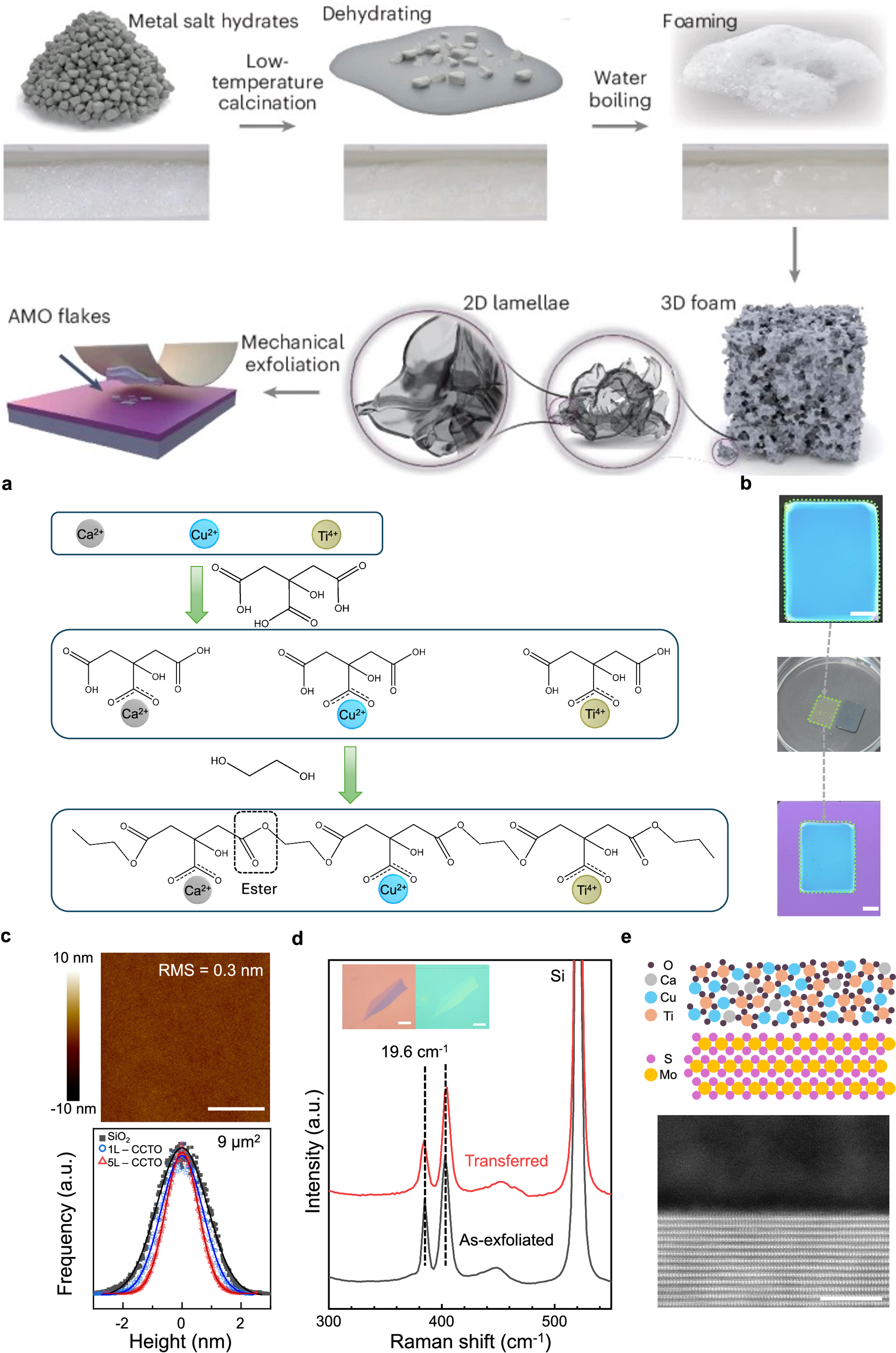
To address the limitations of conventional crystalline gate dielectrics for 2D semiconductor devices, we developed transferable amorphous oxides with enhanced dielectric and multifunctional properties. Traditional methods face challenges in depositing high-k oxides on 2D materials due to their lack of dangling bonds, while existing crystalline dielectrics (e.g., h-BN) suffer from inadequate performance. The research introduces two innovations: (1) A patented "foaming-cleavage" method synthesizes 2D amorphous oxides from metal nitrate foams, enabling scalable production of diverse compositions (seven single-component and multi-component oxides). This process aligns with unconventional fracture mechanics, allowing mechanical thinning without crystallinity constraints. The resulting high-k oxides integrate seamlessly with 2D semiconductors, yielding devices with ultra-low hysteresis (2.7 mV (MV cm⁻¹)⁻¹) (Nat. Synth. 2025, 4, 106). (2) A sol-gel-derived Pechini method produces large-area amorphous CaCuTiO (CCTO) films (k = 42.9) with photosensitivity. Light-induced non-volatile floating-gate effects in CCTO enable nine reconfigurable logic operations (e.g., OR gates) within a single transistor, advancing "sense-memory-compute" integrated devices (Nat. Commun. 2025, 16, 1482).
By overcoming the material and functional constraints of crystalline counterparts, this work establishes amorphous 2D oxides as a versatile platform for next-generation electronics, expanding material diversity, high-performance dielectric integration, and novel optoelectronic applications. These advances pave the way for reconfigurable electronics and multifunctional 2D semiconductor systems.
