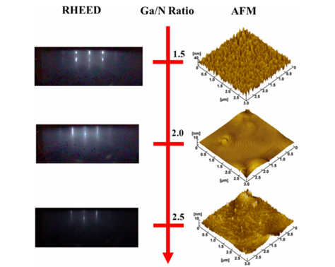
InN has the narrowest bandgap of 0.64 eV at room temperature and the smallest electron effective mass among III-nitrides. The latter leads to much higher electron mobility than GaN and makes InN potentially applicable in high-speed electron devices. In addition, the ternary alloys such as InGaN and InAlN cover a very wide wavelength and thus provide the possibility for the fabrication of many optoelectronic devices such as high-efficiency solar cells and laser diodes in optical communication wavelength range. Our group tries to obtain high-quality InN layers on sapphire substrate by using boundary-temperature-controlled epitaxy.

III-nitrides nanowires (NWs) have attracted tremendous interest in the past decades due to their nearly prefect crystalline quality and a wide range of applications including highly efficient, nanoscale optoelectronic and electronic devices, such as nano-LEDs, nano-LDs, nano-solar cells, single photon emitters, and so on. Single photon emitters hold the promise to serve as quantum bits in quantum communication, linear optical quantum computing and cryptography. Due to thermal and chemical stability, large exciton binding energy, and wide wavelength tunability from the visible to the ultraviolet spectral range, (In,Ga,Al)N quantum dots (QDs) are the most promising candidates for single photon emitting devices. We try to prepare single photon emitters with tunable emission wavelength from visible to infrared spectral range, based on In(Ga)N QD embedded in GaN nanowires structure, and the growth mechanism of nanowires has been analyzed.

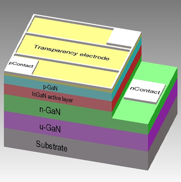
InN, as narrow band gap material in III-N family, has attracted much interest of researchers since its band gap was proved to be about 0.64 eV. The band gap of InGaN material can vary from 0.64 eV (InN) to 3.40 eV (GaN), which covers the whole solar spectrum. InGaN has good match with solar spectrum, direct band gap, big absorption coefficient, good thermal stability and radiation stability, which made it one of the most attractive semiconductor materials for high efficiency solar cell. Unfortunately, high In content InGaN of good quality is still a big challenge due to big lattice difference between InN and GaN. Our group tries to made some efforts to enhance the crystal quality of high In composition InGaN material, such as MQW and InN/GaN short period superlattice (SPSL). On the other hand, we focus on device physics and structure design of the solar cell.

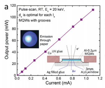
Ultraviolet (UV) light sources with high performance are of great importance due to the various applications. Currently, AlGaN-based UV light sources are considered as the excellent candidates to replace excimer and mercury lamps. Up to date, great progress has been made on this field,however, the output power and emission effiiency of the mid- or deep-UV light sources are still much poorer than those of blue light emitting diodes (LEDs).To overcome some of the issues which limit the output power, we propose, a novel active region, i.e.,quasi-2D GaN layers inserted in AlGaN matrix. Moreover, to avoid the diffiulty in p-type doping of high-Al-content AlGaN and UV light absorption by p-type GaN, an electron-beam (e-beam) pumping method is used instead of conventional electrical injection as reported previously.

UV detector and IR detector are widely used in military and civilian aspects. Integrating the two wavelength(UV-IR) detection can suppress background noise and reduce the false alarm rate,etc. AlGaN-based UV-IR double-color detector show advantages over HgCdTe in terms of the homogeneity, high speed, high integrity, and wide detection range. Besides, the wide bandgap tenability of AlGaN, makes it an unique candidate to realize single-chip monolithic dual-band UV/IR photodetectors. The mid-IR detectors were proposed in our group by AlGaN QWs , by AlGaN step-QWs, and by InGaN QWs. We also engaged in IR detectors from semi-polar QWs based on GaN nanocolumns.

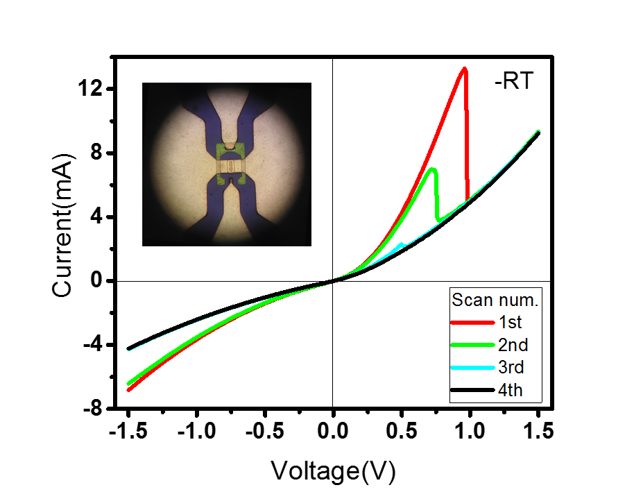
Resonant-tunneling diode (RTD) is a diode with a resonant-tunneling structure in which electrons can tunnel through some resonant states at certain energy levels. The current–voltage characteristic often exhibits negative differential resistance(NDR)regions. One area of active research is directed toward building oscillators and switching devices that can operate at terahertz frequencies. Advances in the MBE technique led to observation of NDR at terahertz frequencies. Specifically, wide bandgap, large conduction band discontinuity ~2.1 eV in AlN/GaN, high carrier mobility, and thermal stability promise high power, high frequency room-temperature operation for GaN-based RTDs. Besides most of semiconductor optoelectronics use III-V semiconductors and so it is possible to combine III-V RTDs to make Optoelectronic Integrated Circuits. Thereby our group focus on high reliability and reproducibility GaN-based RTD deviced.
